- 您现在的位置:买卖IC网 > Sheet目录1999 > ICS9DB202CFLF (IDT, Integrated Device Technology Inc)IC JITTER ATTENUATOR 20-SSOP
CS5532/34-BS
10
DS755F3
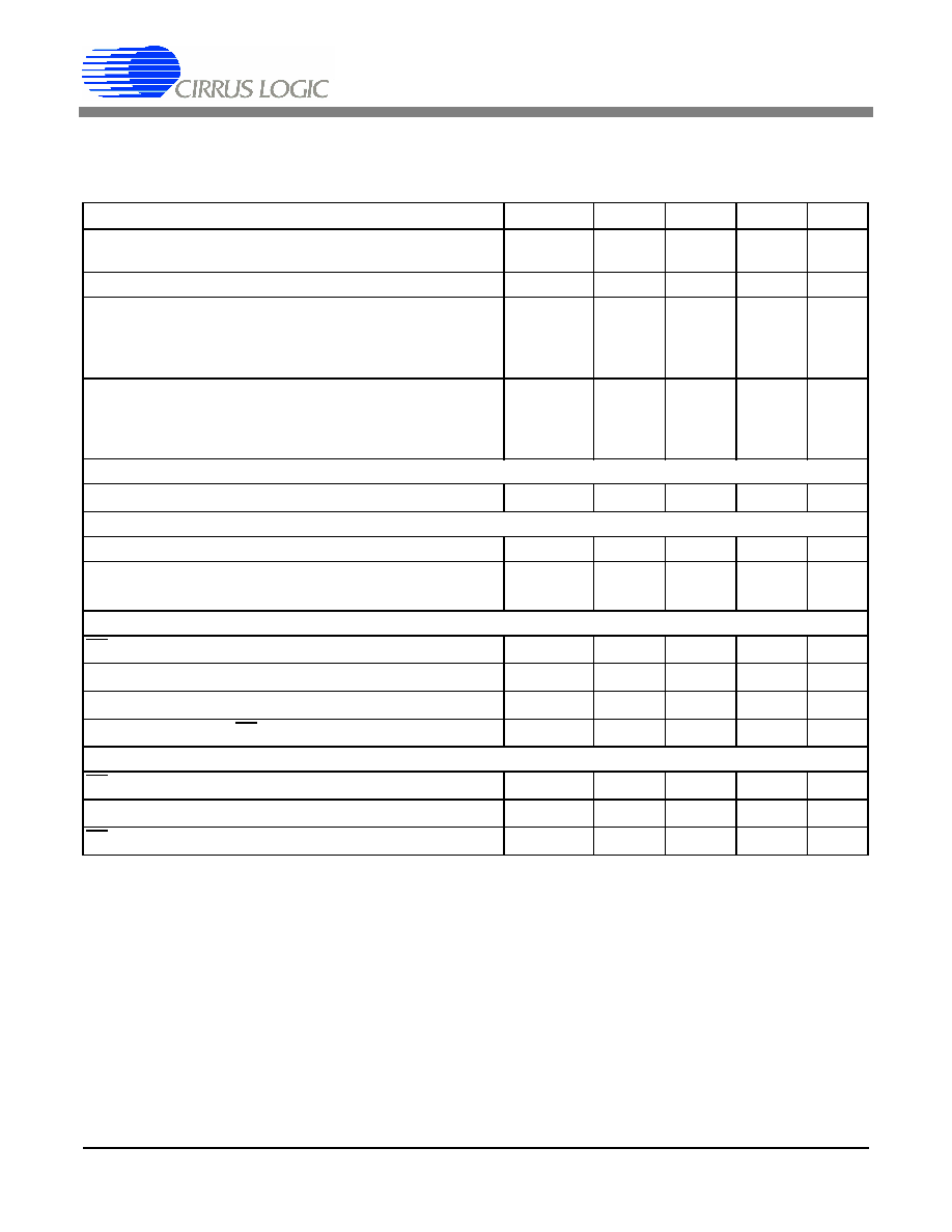
SWITCHING CHARACTERISTICS
(VA+ = 2.5 V or 5 V ±5%; VA- = -2.5V±5% or 0 V; VD+ = 3.0 V ±10% or 5 V ±5%;DGND = 0 V; Levels: Logic 0 = 0
Notes: 27. Device parameters are specified with a 4.9152 MHz clock.
28. Specified using 10% and 90% points on waveform of interest. Output loaded with 50 pF.
29. Oscillator start-up time varies with crystal parameters. This specification does not apply when using an
external clock source.
Parameter
Symbol
Min
Typ
Max
Unit
Master Clock Frequency
(Note 27)
External Clock or Crystal Oscillator
MCLK
1
4.9152
5
MHz
Master Clock Duty Cycle
40
-
60
%
Rise Times
(Note 28)
Any Digital Input Except SCLK
SCLK
Any Digital Output
trise
-
50
1.0
100
-
s
ns
Fall Times
(Note 28)
Any Digital Input Except SCLK
SCLK
Any Digital Output
tfall
-
50
1.0
100
-
s
ns
Start-up
Oscillator Start-up Time
XTAL = 4.9152 MHz
(Note 29)
tost
-20-
ms
Serial Port Timing
Serial Clock Frequency
SCLK
0
-
2
MHz
Serial Clock
Pulse Width High
Pulse Width Low
t1
t2
250
-
ns
SDI Write Timing
CS Enable to Valid Latch Clock
t3
50
-
ns
Data Set-up Time prior to SCLK rising
t4
50
-
ns
Data Hold Time After SCLK Rising
t5
100
-
ns
SCLK Falling Prior to CS Disable
t6
100
-
ns
SDO Read Timing
CS to Data Valid
t7
--
150
ns
SCLK Falling to New Data Bit
t8
--
150
ns
CS Rising to SDO Hi-Z
t9
--
150
ns
发布紧急采购,3分钟左右您将得到回复。
相关PDF资料
ICS9DB202CK-01LFT
IC JITTER ATTENUATOR 32-VFQFPN
ICS9DB206CLLF
IC JITTER ATTENUATOR 28-TSSOP
ICS9DB306BLLFT
IC JITTER ATTENUATOR 28-TSSOP
ICS9E4101AFILFT
IC TIMING CTRL HUB PROG 56SSOP
ICS9EX21801AKLF
IC FANOUT BUFF DIFF 72-VFQFN
ICS9EX21831AKLF
IC FANOUT/BUFFER DIFF 72VFQFN
ICS9FG1901HKLFT
IC FREQUENCY GENERATOR 72-QFN
ID82C54
IC OSC PROG TIMER 8MHZ 24DIP
相关代理商/技术参数
ICS9DB202CFLFT
功能描述:IC JITTER ATTENUATOR 20-SSOP RoHS:是 类别:集成电路 (IC) >> 时钟/计时 - 专用 系列:HiPerClockS™, PCI Express® (PCIe) 标准包装:1,500 系列:- 类型:时钟缓冲器/驱动器 PLL:是 主要目的:- 输入:- 输出:- 电路数:- 比率 - 输入:输出:- 差分 - 输入:输出:- 频率 - 最大:- 电源电压:3.3V 工作温度:0°C ~ 70°C 安装类型:表面贴装 封装/外壳:28-SSOP(0.209",5.30mm 宽) 供应商设备封装:28-SSOP 包装:带卷 (TR) 其它名称:93786AFT
ICS9DB202CGLF
功能描述:IC JITTER ATTENUATOR 20-TSSOP RoHS:是 类别:集成电路 (IC) >> 时钟/计时 - 专用 系列:HiPerClockS™, PCI Express® (PCIe) 标准包装:1 系列:- 类型:时钟/频率发生器,多路复用器 PLL:是 主要目的:存储器,RDRAM 输入:晶体 输出:LVCMOS 电路数:1 比率 - 输入:输出:1:2 差分 - 输入:输出:无/是 频率 - 最大:400MHz 电源电压:3 V ~ 3.6 V 工作温度:0°C ~ 85°C 安装类型:表面贴装 封装/外壳:16-TSSOP(0.173",4.40mm 宽) 供应商设备封装:16-TSSOP 包装:Digi-Reel® 其它名称:296-6719-6
ICS9DB202CGLFT
功能描述:IC JITTER ATTENUATOR 20-TSSOP RoHS:是 类别:集成电路 (IC) >> 时钟/计时 - 专用 系列:HiPerClockS™, PCI Express® (PCIe) 标准包装:1,500 系列:- 类型:时钟缓冲器/驱动器 PLL:是 主要目的:- 输入:- 输出:- 电路数:- 比率 - 输入:输出:- 差分 - 输入:输出:- 频率 - 最大:- 电源电压:3.3V 工作温度:0°C ~ 70°C 安装类型:表面贴装 封装/外壳:28-SSOP(0.209",5.30mm 宽) 供应商设备封装:28-SSOP 包装:带卷 (TR) 其它名称:93786AFT
ICS9DB202CK-01LF
功能描述:IC JITTER ATTENUATOR 32-VFQFN RoHS:是 类别:集成电路 (IC) >> 时钟/计时 - 专用 系列:HiPerClockS™, PCI Express® (PCIe) 标准包装:1 系列:- 类型:时钟/频率发生器,多路复用器 PLL:是 主要目的:存储器,RDRAM 输入:晶体 输出:LVCMOS 电路数:1 比率 - 输入:输出:1:2 差分 - 输入:输出:无/是 频率 - 最大:400MHz 电源电压:3 V ~ 3.6 V 工作温度:0°C ~ 85°C 安装类型:表面贴装 封装/外壳:16-TSSOP(0.173",4.40mm 宽) 供应商设备封装:16-TSSOP 包装:Digi-Reel® 其它名称:296-6719-6
ICS9DB202CK-01LFT
功能描述:IC JITTER ATTENUATOR 32-VFQFPN RoHS:是 类别:集成电路 (IC) >> 时钟/计时 - 专用 系列:HiPerClockS™, PCI Express® (PCIe) 标准包装:1,500 系列:- 类型:时钟缓冲器/驱动器 PLL:是 主要目的:- 输入:- 输出:- 电路数:- 比率 - 输入:输出:- 差分 - 输入:输出:- 频率 - 最大:- 电源电压:3.3V 工作温度:0°C ~ 70°C 安装类型:表面贴装 封装/外壳:28-SSOP(0.209",5.30mm 宽) 供应商设备封装:28-SSOP 包装:带卷 (TR) 其它名称:93786AFT
ICS9DB206CFLF
功能描述:IC JITTER ATTENUATOR 28-SSOP RoHS:是 类别:集成电路 (IC) >> 时钟/计时 - 专用 系列:HiPerClockS™, PCI Express® (PCIe) 标准包装:1 系列:- 类型:时钟/频率发生器,多路复用器 PLL:是 主要目的:存储器,RDRAM 输入:晶体 输出:LVCMOS 电路数:1 比率 - 输入:输出:1:2 差分 - 输入:输出:无/是 频率 - 最大:400MHz 电源电压:3 V ~ 3.6 V 工作温度:0°C ~ 85°C 安装类型:表面贴装 封装/外壳:16-TSSOP(0.173",4.40mm 宽) 供应商设备封装:16-TSSOP 包装:Digi-Reel® 其它名称:296-6719-6
ICS9DB206CFLFT
功能描述:IC JITTER ATTENUATOR 28-SSOP RoHS:是 类别:集成电路 (IC) >> 时钟/计时 - 专用 系列:HiPerClockS™, PCI Express® (PCIe) 标准包装:1,500 系列:- 类型:时钟缓冲器/驱动器 PLL:是 主要目的:- 输入:- 输出:- 电路数:- 比率 - 输入:输出:- 差分 - 输入:输出:- 频率 - 最大:- 电源电压:3.3V 工作温度:0°C ~ 70°C 安装类型:表面贴装 封装/外壳:28-SSOP(0.209",5.30mm 宽) 供应商设备封装:28-SSOP 包装:带卷 (TR) 其它名称:93786AFT
ICS9DB206CLLF
功能描述:IC JITTER ATTENUATOR 28-TSSOP RoHS:是 类别:集成电路 (IC) >> 时钟/计时 - 专用 系列:HiPerClockS™, PCI Express® (PCIe) 标准包装:1,500 系列:- 类型:时钟缓冲器/驱动器 PLL:是 主要目的:- 输入:- 输出:- 电路数:- 比率 - 输入:输出:- 差分 - 输入:输出:- 频率 - 最大:- 电源电压:3.3V 工作温度:0°C ~ 70°C 安装类型:表面贴装 封装/外壳:28-SSOP(0.209",5.30mm 宽) 供应商设备封装:28-SSOP 包装:带卷 (TR) 其它名称:93786AFT